Page Title
This is a Paragraph. Click on "Edit Text" or double click on the text box to start editing the content and make sure to add any relevant details or information that you want to share with your visitors.
DRS4
The DRS4 chip is a full custom Integrated Circuit developed at PSI, Switzerland. It contains a switched capacitor array (SCA) with 1024 cells, capable of digitizing eight analog signals with high speed (6 GSPS) and high accuracy (11.5 bit SNR) on a single chip. This web site contains the chip documentation and software (firmware, drivers, applications) needed in order to work with the chip or the chip evaluation board.
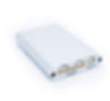
In order to get used to the DRS4 chip, we offer an evaluation board. This board contains following components:
-
Four 50-Ohm terminated input channels with SMA connectors.
-
Active input buffers which result in an analog bandwidth of 700 MHz (-3dB).
-
High bandwidth analog switches for internal voltage calibration.
-
Precision clock for internal timing calibration, reaching a precision of a few pico seconds.
-
One DRS4 chip, capable of sampling the four input signals simultaneously from 0.7 GSPS to 5 GSPS with 1024 sampling points each.
-
One AD9245 ADC to digitize signals from the DRS4 chip.
-
One Xilinx Spartan 3 FPGA for readout control.
-
A 16-bit DAC to generate all on-board control voltages.
-
A serial EEPROM containing serial number and calibration information.
-
Internal trigger with user-defined thresholds on any of the four channels.
-
Triggering on combinations of the four channels (AND/OR) for coincidence measurements.
-
An external trigger input (TTL input 50 Ohm terminated) with a MCX connector.
-
Trigger output for daisy-chaining of several evaluation boards.
-
Clock input and output connectors (MCX) for synchronizing several evaluation boards.
-
A USB 2.0 interface for data readout. This interface also powers this board. The maximum readout rate is about 500 events per second.
-
Several headers for debugging of all important control signals with an oscilloscipe or logic analyzer.
DRS4 ver. 5.1 Software
To download the software please visit the PSI web page.

DRS4 Chip
The DRS chip is a full custom Integrated Circuit developed at PSI, Switzerland. It contains a switched capacitor array (SCA) with 1024 cells, capable of digitizing eight analog signals with high speed (6 GSPS) and high accuracy (11.5 bit SNR) on a single chip.


DRS4 Evaluation Board
In order to get used to the DRS4 chip, we offer an evaluation board. This board contains following components:
-
Four 50-Ohm terminated input channels with SMA connectors.
-
Active input buffers which result in an analog bandwidth of 700 MHz (-3dB).
-
High bandwidth analog switches for internal voltage calibration.
-
Precision clock for internal timing calibration, reaching a precision of a few pico seconds.
-
One DRS4 chip, capable of sampling the four input signals simultaneously from 0.7 GSPS to 5 GSPS with 1024 sampling points each.
-
One AD9245 ADC to digitize signals from the DRS4 chip.
-
One Xilinx Spartan 3 FPGA for readout control.
-
A 16-bit DAC to generate all on-board control voltages.
-
A serial EEPROM containing serial number and calibration information.
-
Internal trigger with user-defined thresholds on any of the four channels.
-
Triggering on combinations of the four channels (AND/OR) for coincidence measurements.
-
An external trigger input (TTL input 50 Ohm terminated) with a MCX connector.
-
Trigger output for daisy-chaining of several evaluation boards.
-
Clock input and output connectors (MCX) for synchronizing several evaluation boards.
-
A USB 2.0 interface for data readout. This interface also powers this board. The maximum readout rate is about 500 events per second.
-
Several headers for debugging of all important control signals with an oscilloscipe or logic analyzer.
By using channel cascading, this board can be configured with 2048 bins for each channel at the expense of a lower analog bandwidth of about 500 MHz. This option has to be requested during an order, since it requires soldering some additional parts. The on-board comparators enables the board to do a self-triggering on a programmed level of any of the input channels or logical combination of channels, much like an oscilloscope. Using the USB 2.0 interface, the evaluation board can be controlled and read out with a maximum rate of about 500 Hz. See the Software Download section for the drivers, firmware and applications for this board.
The external trigger and clock connectors use the MCX standard. Adapters MCX-SMA are available on the market (see DigiKey for example).


